Ministry of Electronics & IT
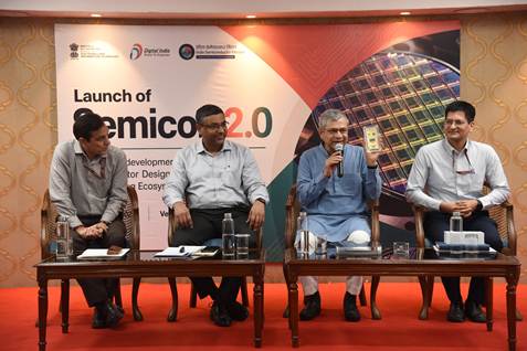
Union Minister Ashwini Vaishnaw addressed media on Semicon 2.0
Notifications for all 6 Pillars of Semicon 2.0 issued
India achieved target of developing 85,000 semiconductor engineers in four years against 10-year target: Ashwini Vaishnaw
Close to 10% of the global semiconductor industry’s market will be in India in the coming years: Ashwini Vaishnaw
Students from Tier-II and Tier-III cities have designed more than 250 semiconductor chips: Ashwini Vaishnaw
Posted On:
31 AUG 2026 4:12PM by PIB Delhi
Union Minister for Electronics and Information Technology, Railways and Information & Broadcasting, Shri Ashwini Vaishnaw, today addressed the media and outlined the Government’s vision for taking India’s semiconductor ecosystem to the next level. On the occasion, notifications for all six pillars of the Semicon 2.0 Scheme were issued, marking a significant step towards strengthening India’s semiconductor design and manufacturing capabilities.
The scheme builds on the momentum generated by the first Semicon India Programme and provides fiscal and infrastructure support across the semiconductor value chain from chip design, fabrication and packaging to equipment, materials, research and development, and talent development.
The scheme aims to strengthen India’s economic growth and national security by improving semiconductor supply-chain resilience and establishing technological leadership in critical sectors. It will operate through six pillars covering 10 categories.
The six pillars under Semicon 2.0 are:
• Pillar 1 - Design
• Pillar 2 - Machines and Materials
• Pillar 3 - Setting up more Fabs
• Pillar 4 - Further strengthening the ATMP/OSAT industry
• Pillar 5 - Research and Development
• Pillar 6 - Talent Development
Pillar 1 - Design: Categories: Design of Semiconductor IPs, Chips, System-on-Chips (SoCs), and Modules for National Importance and Strategic Priorities; Design of Semiconductor IPs, Chips and SoCs for the Commercial Sector; and Deployment-Linked Incentive (DLI) for Semiconductor IPs/Chips/SoCs for deployment.
Pillar 2 - Machines and Materials: Category: Semiconductor manufacturing ecosystem.
Pillar 3 - Setting up more Fabs: Categories: Silicon Semiconductor Wafer Fabs; Compound Semiconductors/Photonics/Sensors (including MEMS) Fab/Discrete Semiconductors Fab; and Display Fabs.
Pillar 4 - Further strengthening the ATMP/OSAT industry: Category: Semiconductor Assembly, Testing, Marking and Packaging (ATMP) / Outsourced Semiconductor Assembly and Test (OSAT) Facility.
Pillar 5 - Research and Development: Category: R&D for advanced semiconductor technologies.
Pillar 6 - Talent Development: Category: Talent Development.
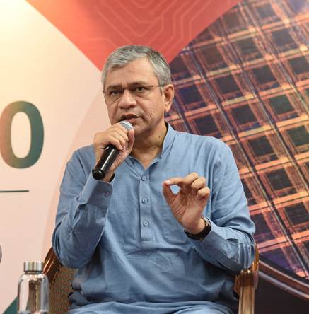
During the event Shri Ashwini Vaishnaw said “India achieved its target of developing 85,000 semiconductor engineers over a period of 10 years in just four years, and has now set a new target of developing one lakh more engineers. In the coming years, close to 10% of the global semiconductor industry’s market is expected to be in India. Students from Tier-II and Tier-III cities have already designed more than 250 chips. In one case, commercial production commenced within just 13 months of the groundbreaking, while approvals were granted within 200 days, 150 days and even 90 days in multiple cases. The semiconductor ecosystem being developed in India is also expected to create 50,000–60,000 direct jobs.”
Projects supported under Semicon 2.0 will generally have a duration of up to six years, while the scheme will initially remain open for applications for three years.
The India Semiconductor Mission (ISM) will be the nodal agency for Semicon 2.0. It will invite applications, undertake technical and financial appraisal, recommend applicants and oversee implementation. ISM may implement the design and deployment categories with the assistance of C-DAC. The mission may also announce semiconductor deep-tech awards from 2026 to promote niche innovation.
The Ministry of Electronics and Information Technology will make budgetary provisions for fiscal support, with disbursements undertaken by the nodal agency in accordance with approved conditions. A mid-term assessment will be conducted after three years of implementation, or as required, to evaluate the scheme’s impact and consider modifications or continuation.
For the notification, you can visit Semicon 2.0
You can watch the Press Conference here
*****
Vinod Kumar/Vanshita Jaiswal/Aparajita Priyadarshini
(Release ID: 2304963)
Visitor Counter : 3418
Read this release in:
Urdu
,
हिन्दी
,
Marathi
,
Assamese
,
Bengali
,
Bengali-TR
,
Punjabi
,
Gujarati
,
Odia
,
Tamil
,
Telugu
,
Kannada