PIB Backgrounder
Chips to Start-up (C2S) Programme
Fostering India’s Indigenous Chip Design Ecosystem
प्रविष्टि तिथि:
18 JAN 2026 9:53AM by PIB Delhi
Key Takeaways
- Over 1 lakh individuals have enrolled in chip design training, with approximately 67,000 trained so far.
- The ChipIN Centre conducted 6 shared wafer runs and 265+ training sessions in collaboration with industry partners.
- The Semi-Conductor Laboratory (SCL) enabled hands-on chip design at scale, with 122 submissions from 46 institutions, including 56 student-designed chips successfully fabricated, packaged, and delivered.
- Participating institutions have filed 75+ patents and are developing 500+ IP cores, ASICs and SoC designs.
Introduction
India is strengthening its semiconductor ecosystem as a strategic pillar of economic growth, technological capability, and national resilience. With global demand for advanced electronics and AI-driven applications rising steadily, the semiconductor industry is projected to reach nearly USD 1 trillion by 2030. At present, the global semiconductor workforce faces a shortfall of semiconductor talent, resulting in a requirement for over 1 million additional skilled professionals by 2032. This positions India as a pivotal contributor to the global semiconductor ecosystem through targeted initiatives.
Recognizing chip design as a strategic national priority, the Ministry of Electronics and Information Technology (MeitY) has implemented proactive measures to transform India’s semiconductor design landscape. These initiatives span approximately 400 organizations, including 305 academic institutions under the Chips to Start-up (C2S) Programme and 95 startups under the Design Linked Incentive (DLI) Scheme.

By enabling nationwide participation in semiconductor chip design, the C2S Programme democratises access to advanced design capabilities. It empowers students, researchers, and entrepreneurs irrespective of institution or location to develop innovative semiconductor solutions, and accelerating indigenous innovation in line with the vision of technological self-reliance and global competitiveness.
Overview: Chips to Start-up (C2S) Programme
The C2S Programme is an umbrella capacity-building initiative launched by the MeitY in 2022, with a total outlay of ₹250 crore over five years, covering academic institutions across India.
The C2S Programme targets the development of 85,000 industry-ready professionals across undergraduate, postgraduate, and doctoral levels. This includes:
- 200 PhD scholars engaged in advanced research in chip design,
- 7000 M. Tech graduates specializing in VLSI or Embedded Systems,
- 8800 M. Tech graduates from computer, communication, or electronic systems programmes with focused VLSI exposure,
- 69,000 B. Tech students trained through VLSI-oriented coursework. Top of Form
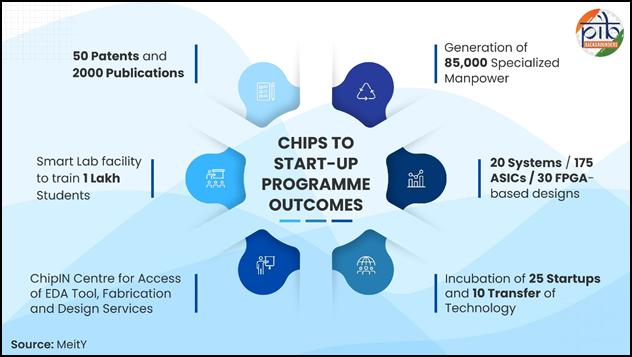
Moreover, beyond manpower generation, the C2S Programme aims to catalyse the incubation of 25 start-ups and enable 10 technology transfers. The programme also seeks to provide access to SMART lab facilities, train one lakh students, generate 50 patents, and support at least 2,000 focused research publications.
This integrated approach of the C2S programme supports innovation, enhances employability, and enables academic institutions to play a more active role in India’s semiconductor value chain. This programme is a strong foundation for self-reliance, innovation, and global competitiveness in the semiconductor sector.
Programme Approach and Implementation
The C2S Programme adopts a comprehensive approach, providing students with hands-on experience in chip design, fabrication, and testing. This is achieved through regular training sessions in collaboration with industry partners, combined with mentorship and practical support. Students gain access to advanced chip design tools, fabrication facilities, and testing resources, including state-of-the-art EDA software and semiconductor foundries, enabling them to design, build, and test their own chips. These opportunities also include implementing R&D projects under the C2S Programme to develop working prototypes of Application-Specific Integrated Circuit (ASICs), Systems-on-Chip (SoCs), and Intellectual Property (IP) Core designs. This structured exposure bridges academic learning with practical semiconductor design and development workflows.
|
Coordinating Organization
|
Mode
|
Area
|
|
100+ Participating Academic Institutions
(Beneficiaries of project funds, EDA Tools & trainings)
|
- Implementation of R&D projects for design & fabrication (2–5 years)
- Instruction as part of curriculum, Short-term courses, labs, and student projects (including nearby institutions).
|
End-to-end exposure to chip design, fabrication, and testing through R&D projects
|
|
200+ Other Organizations
(Beneficiaries of EDA Tools & trainings)
|
Instruction as part of curriculum, Short-term courses, labs, and student projects.
|
General chip design flows using advanced EDA tools.
|
|
ChipIN Centre, C-DAC Bangalore
(Serving 300+ institutions)
|
Regular training sessions with industry partners. Facilities include:
|
Specialized design areas using advance tools.
|
|
EDA tools
|
Synopsys, Cadence, IBM, Siemens EDA, Ansys, Keysight Technologies, Silvaco, AMD, Renesas
|
|
Foundry access
|
SCL, IMEC, MUSE Semiconductors
|
|
Chip design flow
|
ChipIN Centre, NIELIT
|
|
SMART Lab, NIELIT Calicut (Pan-India institutions)
|
Identified short-term and certification courses.
|
General chip design flows using centralized hardware resources.
|
This integrated approach ensures that students and institutions can develop working chip designs, system-level chips, and reusable design blocks, while promoting innovation through patents, technology transfers, and start-up incubation.
ChipIN Centre: Enabling Chip Design and Fabrication Support under C2S Programme
The ChipIN Centre at C-DAC Bengaluru is one of India’s largest facilities providing shared semiconductor design infrastructure to academic institutions and startups across the country. It offers access to advanced chip design tools covering the entire design cycle, along with compute and hardware infrastructure, intellectual property cores, and technical mentorship. This centralized support enables institutions to undertake chip design and fabrication activities, strengthening India’s domestic semiconductor design capability.
Role of ChipIN Centre Under the C2S Programme
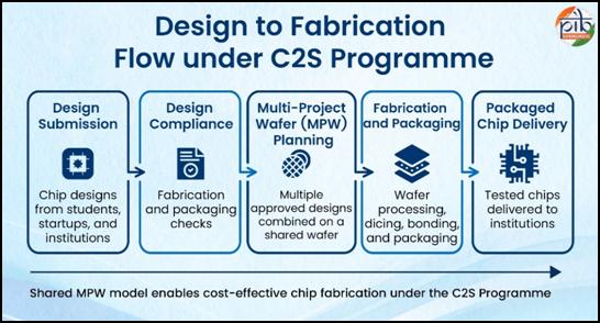
- Design Collection and Fabrication: The ChipIN Centre collects chip designs created by students from C2S Programme institutions. Every three months, these designs are grouped together and sent to Semi-Conductor Lab (SCL) Mohali for fabrication using 180 nm technology.
- Design Verification: The ChipIN Centre checks whether the designs meet fabrication requirements and works with students to improve them through feedback and revisions. Once approved, the designs are combined onto a single shared wafer by the Centre. The shared wafer is sent to SCL Mohali. SCL Mohali fabricates, packages, and delivers the chips back to the students.
- Technical Support: The ChipIN Centre provides centralized technical support to students at participating institutions. Over the past few years, 4,855 support requests have been addressed by the ChipIN Centre.
Key Outcomes of the C2S programme
The Chips to Start-up Programme has delivered measurable outcomes across capacity building, infrastructure access, and hands-on chip design enablement. Through a combination of national technological facilities and fabrication support, the programme has enabled large-scale participation from academic institutions and startups.
- Around 1 lakh individuals from 400 organisations, including 300 academic institutions and 95 startups have used shared national EDA infrastructure resulting in more than 175 lakh hours of tool usage.
- 6 shared wafer runs were organised by the ChipIN Centre during the past years at Semi-Conductor Laboratory, Mohali, enabling 122 chip design submissions from 46 institutions.
- A total of 56 student-designed chips were successfully fabricated, packaged, and delivered.
- 265+ industry-led training sessions were conducted across key chip design domains for students, researchers, and engineers.
- Participating institutions have filed over 75+ patents across chip design and semiconductor manufacturing workflows.
- Institutions are developing 500+ IP cores, Application Specific Integrated Circuits and System-on-Chip designs for use in defence, telecom, automotive, consumer electronics, and industrial applications.
- Centralised and distributed Field Programmable Gate Array (FPGA) boards were provided to participating institutions to support hands-on learning, design validation, and prototyping activities.
- High-performance computing access was provided through the PARAM Utkarsh supercomputer.
Institutional Framework Supporting the C2S Programme
India’s chip design ecosystem under the Chips to Start-up Programme is being strengthened through a coordinated institutional framework that combines technological infrastructure support and large-scale capacity building. Key programmes and institutions such as C-DAC and ChipIN centre, provide end-to-end enablement for chip design education and innovation. By integrating R&D institutions and industry partners, the C2S institutional framework supports indigenous chip design and advances India’s objective of a self-reliant and globally competitive semiconductor design ecosystem.
Ministry of Electronics and IT (MeitY)
MeitY leads national semiconductor initiatives, provides policy direction, and anchors schemes such as Chips to Start-up Programme. It also coordinates institutional and industry partnerships to strengthen India’s chip design and manufacturing ecosystem. MeitY provides overall policy direction, funding support, and programme oversight for C2S. It aims to offset the existing disabilities in India’s domestic semiconductor design industry. It seeks to help Indian companies move up the semiconductor value chain.
Centre for Development of Advanced Computing (C-DAC)
C-DAC has established and operates the ChipIN Centre at Bengaluru, which serves as the national hub for chip design enablement. The Centre provides shared access to commercial EDA tools, high-performance computing resources, IP libraries, and technical mentoring. It also manages design onboarding, verification, and aggregation for fabrication.
Semi-Conductor Laboratory (SCL), Mohali
Under the Chips to Start-up Programme, SCL facilitates fabrication of chip designs developed by students and researchers from participating academic institutions through shared wafer runs. SCL undertakes fabrication using established process technologies and provides packaging support for approved designs. Fabricated chips are delivered back to institutions, allowing students to validate designs on silicon and gain practical exposure to post-fabrication testing and evaluation.
These coordinated institutional frameworks ensure equitable access to national chip design infrastructure, strengthens academia–industry collaboration, and builds a steady pipeline of industry-ready chip designers. It plays a critical role in advancing indigenous chip design capability and positioning India as a credible participant in the global semiconductor ecosystem.
Conclusion
Semiconductors have emerged as a strategic foundation for innovation, economic growth, and national security. Leadership in semiconductor design and talent development is increasingly central to global technological competitiveness. Recognising this, India is positioning its academic and innovation ecosystem to play a decisive role in shaping future semiconductor technologies.
The Chips to Start-up Programme reflects India’s commitment to building a strong and self-reliant semiconductor ecosystem. By enabling large-scale skill development, hands-on design experience, and access to national infrastructure, the programme is empowering students, researchers, startups, and entrepreneurs to contribute to indigenous chip design and innovation. These efforts are strengthening India’s talent base, supporting technological self-reliance, and advancing the country’s journey towards becoming a globally competitive hub for semiconductor design and development.
References
Ministry of Electronics and IT - Chips of Start-up Programme Portal
Press Information Bureau
Ministry of Skill Development and Entrepreneurship
Kindly click here for PDF
***
PIB Research Unit
(रिलीज़ आईडी: 2215755)
आगंतुक पटल : 8544