Ministry of Science & Technology
New Artificial Nanostructures for Infrared Absorption Technologies can be useful in Defense, Imaging & Sensing
Posted On:
24 DEC 2022 11:35AM by PIB Delhi
A new method to confine and absorb infrared (IR) light with GaN nanostructures can help develop highly efficient infrared absorbers, emitters, and modulators that are useful in defense technologies, energy technologies, imaging, sensing, and so on.
GaN, a widely used material for blue light emission, is one of the most advanced semiconductors. Though visible and ultraviolet light applications of GaN have already been realized, with LEDs and laser diodes commercially available, utilization of GaN for IR light harvesting or development of GaN-based IR optical elements is lacking.
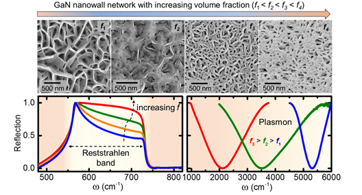
Researchers in Bengaluru’s Jawaharlal Nehru Centre for Advanced Scientific Research (JNCASR), an autonomous institute of the Department of Science and Technology, have shown for the first time infrared light emission and absorption with GaN nanostructures. Though blue light emission from GaN has been known for some time, and it is used in LEDs, this is the first time that infrared light-matter interactions are demonstrated in GaN. For this demonstration, they have utilized a scientific phenomenon called surface polariton excitations in GaN nanostructures that lead to light-matter interactions at IR spectral range.
Surface polaritons are special modes of electromagnetic waves traveling at the interface of a conductor and an insulator such as air. By altering the morphology and shape of the nanostructures, they are also able to excite plasmon polaritons in GaN, which results in extending the light-matter coupling to further reaches of the electromagnetic spectrum. These polaritons are quasi-particles which have both light and matter characteristics.
To grow these GaN nanostructures, the researchers utilized a specialized material deposition instrument called molecular beam epitaxy in the International Centre for Materials Science in JNCASR. This instrument uses ultra-high vacuum, similar to the conditions of outer space, to grow high-quality material nanostructures with dimensions about 100000 times smaller than the width of a human hair.
Such cutting-edge materials allow the creation of polariton-based devices, which offer several advantages to conventional electronic devices. Polaritonic technologies have attracted a wide range of applications, such as secure high-speed light-based communication (LiFi), next-generation light sources, solar energy converters, quantum computers, and waste-heat converters.
“In the last 25 years, blue LED with GaN has changed our world significantly. While the blue light emission from GaN is well-understood, utilizing GaN for infrared optics is not well-established. Our work demonstrates a novel pathway for utilizing GaN in infrared nanophotonic applications. Importantly, the scientists said that the infrared surface polariton excitations that we have demonstrated can be translated to many other semiconductors as well”. The research has been published in the prestigious journal Nano Letters. The proof of concept of the technology has been demonstrated.
“This work will greatly benefit in addressing the demand for IR sources and detectors for energy, security, imaging, and other applications,” said Dr. Bivas Saha, Assistant Professor at the Jawaharlal Nehru Centre for Advanced Scientific Research.
Publication link:
https://pubs.acs.org/doi/pdf/10.1021/acs.nanolett.2c03748
Nano Letters – Published 2 December 2022
For more details, please contact Dr. Bivas Saha, Email ID: bsaha@jncasr.ac.in , Mobile no.: +91-80-2208-2619.

Figure: Light manipulation via exciting the polaritons in GaN nanostructured. By controlling the morphology of the GaN nanostructures, the polariton excitations are tuned in a controlled way.

<><><>
SNC/RR SNC/RR
(Release ID: 1886246)
Visitor Counter : 2721