Ministry of Science & Technology
New memory device with excellent switching characteristics and low-power requirements developed
Posted On:
15 JUL 2022 4:31PM by PIB Delhi
Scientists have developed a memory device with excellent switching characteristics and low-power requirements for data storage applications.
Resistive memory devices with insulating film sandwiched between electrodes can address the needs of high-performance, and high-density memories with low power requirements for data storage. They are devices with resistive switching characteristics which refers to the physical phenomena in which a dielectric (electrical insulator that can be polarised by an applied electric current) suddenly changes its (two terminal) resistance under the action of a strong current. Though such devices have been studied intensively to meet the huge technological demands in terms of performance, several technical challenges still persist and pose major challenges to their commercialization.
Extensive efforts are being made by scientists to design resistive switching-based memory devices that are non-volatile, reliable, and perform much better than the existing silicon-based flash memory technology.
Ms. Swathi S. P. and Dr. S. Angappane from the Centre for Nano and Soft Matter Sciences (CeNS), Bangalore, an autonomous institution of Department of Science and Technology, Govt. of India (DST), have developed a low-power memory device with excellent switching characteristics made from the chemical hafnium oxide, a replacement for silicon oxide, for data storage applications.

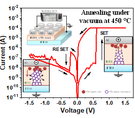
I-V characteristics of a Al/HfOx/FTO device exhibiting the bipolar resistive switching behavior with low set/reset voltages and currents. Insets show the schematic of the device structure and the switching dynamics.
They have used hafnium oxide (HfO2), an insulator which can be polarised on application of electric current as an insulating layer. They prepared with by a method called sputtering deposition method. It is a physical vapour deposition technique in which energetic ions are used to knock off the atoms or molecules from the desired ‘target’ material and deposit them onto a substrate. The HfO2 film’s resistive switching characteristics could further be enhanced by tuning the growth temperature and annealing conditions -- a heat treatment process that changes the physical and sometimes chemical properties of a material to increase ductility and reduce the hardness to make it more workable.
The team found that a higher concentration of oxygen vacancies (loss of oxygen from their respective positions in the crystal lattice) is created when these films are subjected to heat thermal treatment process called annealing. The oxygen vacancies play a vital role in creating conditions for low power operations. Besides, thermal treatment also influenced crystalline behaviour and density of defects of the hafnium oxide films, thereby affecting resistive switching parameters and device performance. Besides, the devices also exhibited good endurance, and high retention.
Their research published in the Journal of Alloys and Compounds can contribute to the development of more efficient, viable, and reliable resistive memory devices in the future. The CeNS researchers are converting these resistive memory devices into miniature forms. The team is investigating brain-inspired functionalities in these memory devices and exploring the possibility of integrating the memory device with other potential sensors to bring out its multifunctional capabilities.
Publication link: 10.1016/j.jallcom.2022.165251
For more details, please contact Dr. S. Angappane (Email: angappane@cens.res.in).
*****
SNC / RR
(Release ID: 1841776)
Visitor Counter : 1873