Ministry of Science & Technology
Unlocking the power of chirality for next-generation optoelectronics
प्रविष्टि तिथि:
19 SEP 2025 4:39PM by PIB Delhi
Exploring chiral perovskite films used in optoelectronic devices, scientists have identified how the materials crystallise for making phase-pure, chiral perovskite films, having unique properties, useful for developing devices like circularly polarized light (CPL) detectors, spintronic elements, and photonic synapses. Such an orientation for chiral perovskite films brings additional control on their electrical properties, making them more versatile.
Chirality – the property of an object being non-superimposable on its mirror image – is found everywhere in nature, from spiral galaxies to the DNA in our cells. In materials science, chirality can enable unique light–matter interactions, such as controlling the spin of electrons or detecting circularly polarized light. These capabilities open the door to futuristic technologies in quantum optoelectronics, advanced sensors, and spin-based computing.
Until now, most chiral materials have been organic, which limits their usefulness in devices because they transport electrical charge poorly. In contrast, halide perovskites – a class of crystalline materials – have emerged as excellent candidates for optoelectronics due to their tunable properties and efficient charge transport. Combining chiral molecules with low-dimensional halide perovskites can create chiral perovskites with enhanced performance.
However, making high-quality chiral perovskite films for devices requires precise control over how they crystallize – something that has remained poorly understood.
Researchers at the Centre for Nano and Soft Matter Sciences (CeNS), Bengaluru, an autonomous institute under the Department of Science and Technology (DST), have now uncovered the detailed crystallization mechanism of such materials. Studying thin films of methylbenzylammonium copper bromide ((R/S-MBA)₂CuBr₄), the team found that the crystallization in these low-dimensional films begins at the air-film interface and proceeds towards the substrate.
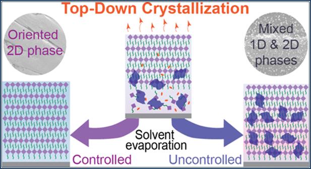
Fig: Controlling the solvent evaporation during the 2D perovskite film processing can provide phase-pure and oriented chiral perovskites.
They also discovered that unwanted 1D impurity phases form due to trapped residual solvent during cooling, which can affect device quality. Importantly, the researchers showed that vacuum processing and careful solvent selection can suppress these impurities, leading to more uniform films. They even tracked crystal growth over two weeks, revealing how small grains evolve into well-organized structures.
This work provides a clear strategy for making phase-pure, oriented chiral perovskite films — a crucial step toward building devices like circularly polarized light (CPL) detectors, spintronic elements, and photonic synapses. The team is now working on fabricating photodetectors based on these films.
With India’s growing research strength and push toward semiconductor and optoelectronic manufacturing, mastering such materials can position the country at the forefront of next-generation light-based and quantum technologies.
***
NKR/PSM
(रिलीज़ आईडी: 2168514)
आगंतुक पटल : 550