Ministry of Science & Technology
Rare electron localization phenomena demonstrated, can expand scope of semiconductors
प्रविष्टि तिथि:
29 AUG 2024 4:23PM by PIB Delhi
Researchers have unveiled a rare type of electron localization phenomenon that can increase the options for material choices and can be used either to improve the existing performances of semiconductors or expand their applications in areas like lasers, optical modulators, and photoconductors.
Anderson Localization of elementary quasiparticles like electrons, photons, and phonons in disordered and amorphous semiconductors, proposed by American theoretical physicist P W Anderson, is an intriguing phenomenon in solid-state physics. It occurs when doping and impurities lead to the absence of conduction in metals or semiconductors.
As a result of doping and impurities, the electrons that otherwise used to travel from a region of high potential to one of low potential in a conducting material, become confused and roam around the doped or the impurity centers. It leads to transition of a -conductor to insulator called Anderson transition.
In contrast to the traditional view of Anderson localization, which emphasizes the importance of geometric or topological defects like vacancies or dislocations (where electrons do not flow) in lattices, theoretical physicists Boris I. Shklovskii and Alex L. Efros proposed that potential fluctuations caused by random distributions of charged dopants could also induce a metal-insulator transition, known as the quasiclassical Anderson transition. Despite decades of effort, direct experimental verification of this phenomenon has remained elusive.
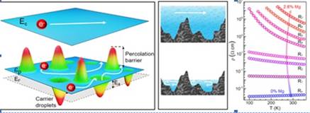
In a significant discovery, researchers at Bengaluru’s Jawaharlal Nehru Centre for Advanced Scientific Research (JNCASR), an autonomous institute of Department of Science and Technology (DST), Government of India, have used oxygen and magnesium as random dopants to demonstrate a quasiclassical Anderson transition that creates fluctuation of potential, (electrical potential) leading to bubbles of electrons inside a dielectric matrix that bring about a band structural change in the parent material. This leads to what is known as the percolative metal-insulator transition -- the structure remain same but electroically there is a transition.
Spearheaded by Associate Professor Bivas Saha, the team unveiled how single-crystalline heavily doped and highly compensated semiconductors undergo a remarkable metal-insulator transition with single crystalline scandium nitride as an example.
This transition published in the journal Physical Review B is accompanied by an astonishing nine orders of magnitude change in resistivity, offering fresh insights into the electron localization behavior in these materials.
The researchers have adopted a unique approach. They utilized a magnesium (hole) compensated scandium nitride semiconductor, and deposited it under ultrahigh vacuum growth conditions. The fluctuating potential within these materials resulted in not just the metal-insulator transition but also anomalous behaviors in carrier mobility, thermopower, and photoconductivity.
The potential fluctuation resulting from the random distribution of the dopants increases the resistivity of the semiconductor by localizing the carriers. The electron transport in such localized systems occurs through a percolation process, which is not very common in semiconductors. Hence the physics explaining the electrical transport and the properties like mobility, photoconductivity, and thermopower are different in such materials.
Dr. Dheemahi, the lead author of the paper, remarked, “Such an electronic transition in single-crystalline and epitaxial semiconductors could open pathways for their utilization in various applications, including lasers, optical modulators, photoconductors, spintronic devices, and photorefractive dynamic holographic media.” Potential fluctuations can be a novel tool to alter semiconducting properties in materials and may lead to more efficient semiconductors in many branches of studies.
“Our research marks the inaugural experimental confirmation of the quasiclassical Anderson transition and percolative metal-insulator transition in materials. We illustrated that potential fluctuations resulting from the random distribution of dopants drastically alter the electron transport physics in semiconductors invoking the percolation process. Moreover, we show that one can achieve a phenomenon that is very similar to the Anderson transition, albeit in a single-crystalline material. These findings are poised to transform our understanding of electron localization in materials.” said Prof. Bivas Saha.
Apart from JNCASR, researchers from the University of Sydney, Australia, and Deutsches Elektronen-Synchrotron, Germany, also participated in this work.
Publication:
https://journals.aps.org/prb/abstract/10.1103/PhysRevB.109.155307
Phys. Rev. B 109, 155307 – Published 25 April 2024
***
KSY/PSM
(रिलीज़ आईडी: 2049764)
आगंतुक पटल : 1544